PCIM Seminar: Innovative Product Development for Power Electronics: Tools, AI and Customer-Centered Solutions
Innovative Product Development for Power Electronics: Tools, AI an...


Metallic sintering with copper or silver pastes has established itself in recent years as a highly reliable alternative to soldering. The pressurized sintering process in particular is orders of magnitude superior to soldering in terms of the maximum possible application temperature and lifetime. However, pressures of 10 MPa to 30 MPa are applied to the semiconductors to create these connections. In addition, precise temperature control and clean surfaces are necessary to process a high-quality sintered connection. Therefore we offer you a comprehensive range of training courses on the sintering process with an overview of the entire production line, as well as workshops on the necessary boundary conditions such as material quality.


Silver-sintered power semiconductors – especially SiC – are now state of the art. Nevertheless, the step from the laboratory to series production is a major challenge. In order to design an economically successful sintering process, reject rates of <5% are required. However, the yield at the start of series production is usually only 50%. A major factor is the sintering knowledge of employees on the line. Due to the new technology, it is difficult to recruit experienced employees. Therefore, a forward-looking and long-term training concept is necessary to make sinter production successful.
However, the selection of suitable machines and processes is extremely important for the success of the sintered product. The purchase price of the production line is less of a priority than its robustness and process quality.
We help you to select the tight production technology, create a training concept with you and train your employees: from operators to management. For existing production lines, we also optimize the process with your engineers and ensure a sustainable transfer of knowledge.
Copper sintering is also part of our expertise. We can help you introduce a cost-effective copper sintering process.
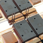
Clip sintering or ribbon sintering is used to replace conventional thick-wire bonds and thus increase the lifetime of the power modules. Aluminum bond wires are the weakest point in active power cycling tests. Sintering ribbons or clips is therefore an alternative. These can either be sintered directly onto the semiconductor and substrate or serve as an intermediate layer for bonding copper wires.
The top side of the semiconductor presents a challenge for the sintering process due to the transistor structures and the sensitive gate oxides. The top side can also be contaminated from previous processes, which means that pre-cleaning using plasma is necessary.
There are also various process routes to realize this connection. These include preforms, films, printing of pastes, pre-amplified sintered paste, dispensing and jetting.
We help you select a suitable material for your product and develop the process together with your engineers.


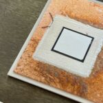
Large-area sintering refers to the bonding of substrates or printed circuit boards to heat sinks or base plates. The surfaces are usually significantly larger than 100mm2. The motivation for choosing a sintered connection is the significantly higher thermal conductivity, temperature capability and thermal shock resistance compared to soldering.
However, the connections are very complex to produce. Due to the curvature of the components, printed layer thicknesses of 200…500µm are necessary to obtain a continuous sintered layer. In addition, the requirements for base plate and cooler surfaces are significantly higher than for soldering. While the solder can compensate for unevenness in the liquid phase, the surface quality must be very closely tolerated during sintering.
In recent years, several process routes have been established for large-area sintering. These include:
We support you in the selection and specification of materials, process development and train your employees in all common process routes.
Pressureless sintering has established itself primarily for small components. These include LEDs with a size of <3x3mm, SMD components or pressureless clip sintering.
There are now various pressureless sintering pastes with silver and copper particles, as well as hybrids filled with epoxy resin or other polymers. The appropriate technology is used depending on the application, lifetime requirements and cost pressure.
Pre-processes are of crucial importance in pressureless sintering. These include dispensing or printing the paste, as well as the precise placement of the components. Normally, the paste is not pre-dried, but will be dried during the sintering process or its profile. For this reason, it is extremely important that the pick&place machine can place the components precisely in the Z-direction. This ensures that the component is not too deep in the paste, but is completely wetted.
We support you in estimating costs and process times, selecting materials and process development in the form of on-site training and assignments.

Originally published by Schwarzbauer 1989, metallic silver sintering has proven to be a much more reliable alternative to soft soldering in power electronics in recent years. In addition to numerous dissertations, a number of industrial companies have also looked into the subject and are using the process in series production.
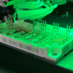
Metallic silver sintering is a solid phase sintering process. Particles are present in paste form together with encapsulating and dispersing agents as well as organic binders. The paste is applied to the substrate by stencil or screen printing or by dispensing and then dried. The chip is then loaded and bonded to the substrate by the silver particles in one to two minutes at pressures of up to 50 MPa and temperatures of 200 °C to 300 °C.
As the sintering reaction takes place well below the melting temperature, the process is also referred to as low-temperature joining technology (LTJT). In most cases, LTJT requires a precious metal surface for the joining partners, whereby pastes for copper surfaces are now state of the art and copper pastes are currently making the leap into series production. Sintered joints show an order of magnitude better load cycle resistance compared to soft solders. The reason for this is the four times higher electrical and thermal conductivity as well as the five times higher yield point and the 15% lower thermal expansion of pure silver compared to SAC solders. At 962 °C, the melting point of silver is significantly higher than that of soft solder alloys. This makes the material ideal for high-temperature applications.

Innovative Product Development for Power Electronics: Tools, AI an...
Development of a sintering process for power modules using the PERFORM method: A practical application.
...
Presentation at the ECPE Hybrid Workshop Sinter Technology in Power El...
Finally, Bond Pulse will offer a public seminar.
...
Our new article on the motivation behind sintering power semiconductors was published today in Semiconductor Packaging News
...